Memory Write access with custom DMA to SDRAM

Memory Write access with custom DMA to SDRAM

by Amaury Pierre Jiezhi Wei -
Number of replies: 9
Hello,

I have a problem with memory write accesses with a custom Avalon Master using the SDRAM controller on the De1-SoC board.

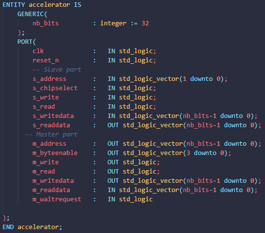
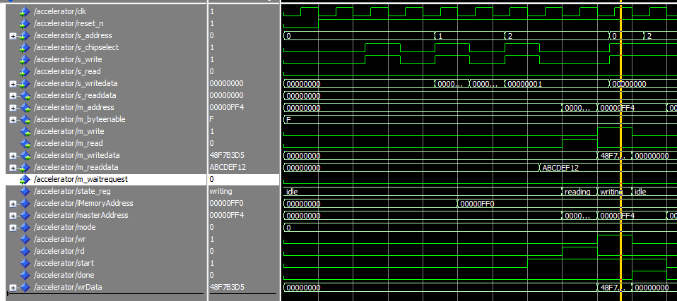
I designed a DMA accelerator to perform the bit/byte reversing/swapping operations as asked in the data. I simulated the design using Modelsim and it works smoothly.

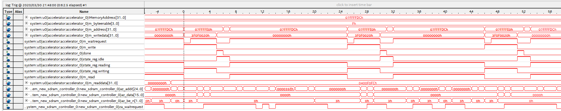
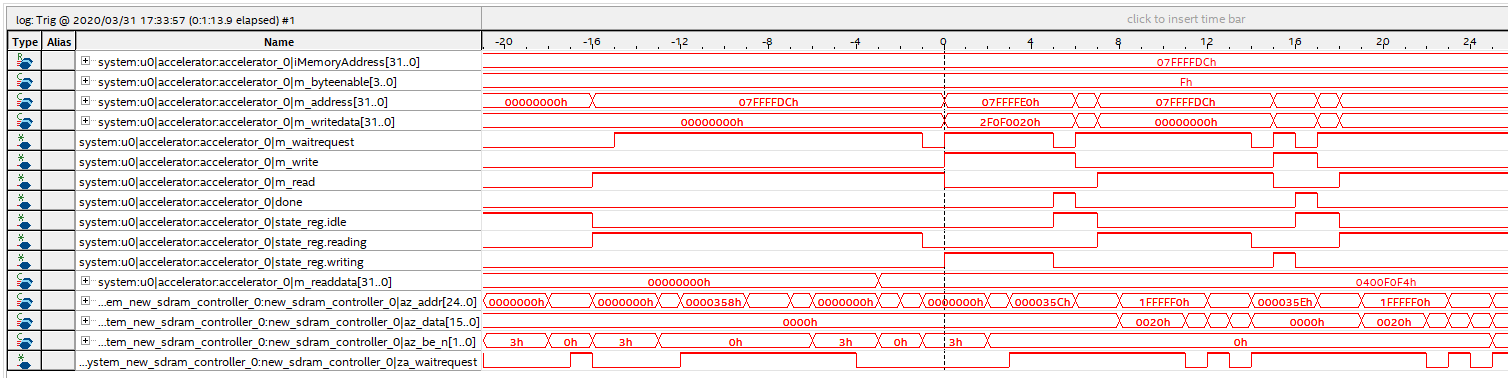
My custom Avalon Master is able to perform a read access in the SDRAM. It can compute the new data from it to write it in the memory. All the signals are asserted at the output of my DMA. However, the data is never written in the SDRAM. When I read the data at the location it is supposed to write to, the DMA has not written anything in the memory.

Do you have an idea what could go wrong when the DMA writes in the memory? The byte_enable signal is set to "1111", I take into account wait_request as well.

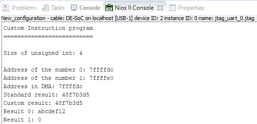
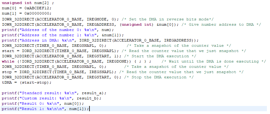
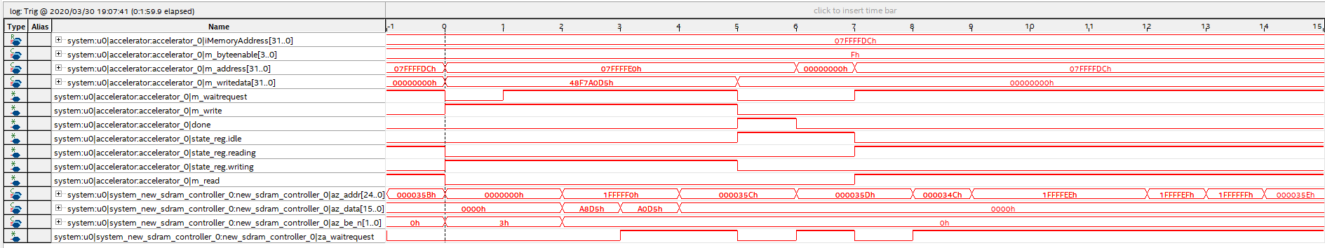
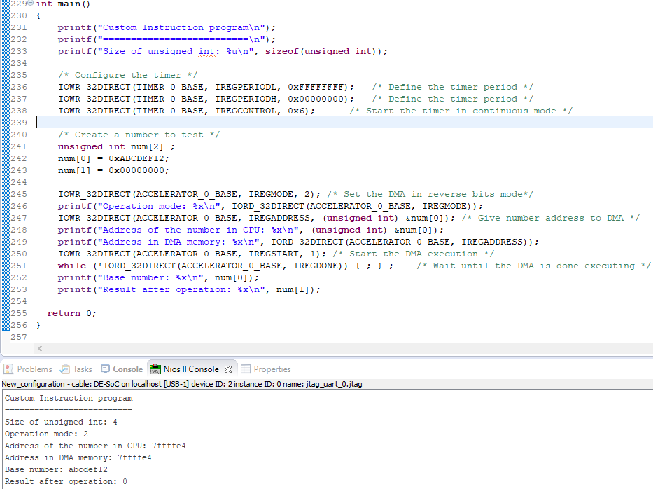
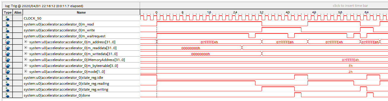
Please find below a code snippet in C and the results in the Nios II console, along with a screenshot of the Signal Tap Analyzer I used to monitor the DMA signals.

Best regards,
Amaury

nios2-console-log

c-code-snippet

signal-tap-logic-analyzer-signals

dma-signals
In reply to Amaury Pierre Jiezhi Wei

Re: Memory Write access with custom DMA to SDRAM

by Sahand Kashani-Akhavan -

Hi,

Based on your vhdl, your accelerator is just reading/writing 1 word, and if I understand correctly, you expect it to flip the bytes of 0xABCDEF12 (i.e. you expect to get 0x21FEDCBA). Is that correct?

One thing that bothers me is how you are setting the target address from which the DMA reads and writes in memory. You are doing &num[0] which gives the address of the table entry in the CPU's address space, but the same variable may not have the same address in the accelerator's address space. Can you take a screenshot of your Qsys system's "address" tab. That would give the answer.

I would have been able to infer if you're reading from memory correctly from the waveforms, but you didn't put the accelerator's read signals, so it isn't possible to confirm my hypothesis. Can you add the bus read signals (m_read, m_readdata) as well?

In reply to Sahand Kashani-Akhavan

Re: Memory Write access with custom DMA to SDRAM

by Amaury Pierre Jiezhi Wei -

Hello,

Thanks for your answer. Actually my DMA can do multiple bit/byte manipulations (I can choose by changing the "IREGMODE" register in the DMA), but in this case I'm expecting to flip all the bits of 0xABCDEF12, which would result in 0x48F7B3D5. When I simulate my component in Modelsim, this is the value I get.

modelsim-simulation

As I obtained a result very similar after computation, I assumed that it can read the memory at this address. However, it looks like it's not the same result I was supposed to get.

After running again the code and adding the two (m_read, m_readdata) signals, I obtained the following result:

stla-error-2

The m_readdata signal is 0x0400F0FC, which after bit flipping, results in 0x3F0F0020 (which is the result sent back by the DMA). However, the  m_readdata signal is not the 0xABCDEF12 I was expecting to find.

Here goes the address map of the system. How can I "translate" the SDRAM address from the CPU point of view to the address from the DMA point of view?

qsys-address-map

Thanks for you help again.

Best regards,

Amaury

In reply to Amaury Pierre Jiezhi Wei

Re: Memory Write access with custom DMA to SDRAM

by Sahand Kashani-Akhavan -

Ok, so the good news is that you are lucky and Qsys is assigning the same address ranges to the SDRAM for both the CPU and the accelerator, so you should be able to just use the number returned by &num[0] as the target address of the accelerator. There is generally no automatic way of doing translation without an MMU or TLB, but we don't have any here. What one could do if there was a mismatch between the address ranges is to put an "Address span extender" in Qsys between the 2 components and offset the addresses that one component sees when it issues addresses.

Signaltap is bad at this because it doesn't show where clock edges are, but based on what I see in your signaltap trace you don't seem to be reading correctly. You have m_read asserted while m_waitrequest is asserted, but you drop m_read as soon as m_waitrequest is 0. Instead, you are supposed to keep m_read asserted until m_waitrequest is deasserted (including the clock cycle where m_waitrequest is deasserted). Basically you need to have m_read = 1 AND m_waitrequest = 0 for the transfer to be accepted by the slave, but you have m_read = 0 AND m_waitrequest = 0 (look at time interval -4 to 1).

As you say you do not get 0xABCDEF12 when reading from the SDRAM and are instead getting some random value 0x0400F0FC. You can tell this is wrong because the value is already on the m_readdata bus before m_waitrequest = 0.

In reply to Sahand Kashani-Akhavan

Re: Memory Write access with custom DMA to SDRAM

by Amaury Pierre Jiezhi Wei -

Thank you for your answer. I see, the address ranges are both the same.

I see, I will try to fix the problem and keep the m_read and m_write signals for one more clock cycle after m_waitrequest is cleared. Thanks!

In reply to Sahand Kashani-Akhavan

Re: Memory Write access with custom DMA to SDRAM

by Amaury Pierre Jiezhi Wei -

I fixed the accelerator to keep the m_read and m_write signals to 1 when wait_request becomes 0, but I still have the same problem.

The readdata signals never changes. Do you have an idea why?

Meanwhile, the accelerator is now writing inside the SDRAM and I can now read the value 2F0F0020 at the address the result is supposed to be. The only problem left is the reading of the data in the SDRAM.

stla-error-3

In reply to Amaury Pierre Jiezhi Wei

Re: Memory Write access with custom DMA to SDRAM

by René Beuchat -

Hello,

You say tham m_readdata is not changing, yes it change:

You want to make the conversion:

0x AB CD EF 12 --> 0x 12 F7 B3 AB 

1100 1101 1110 1111 (CD EF) --> 1111 0111 1011 0011 (F7 B3)


In your timing diagram, you read @ address 0x 07FF FFDC : 0x 04 00 F0 F4

0000 0100 0000 0000 1111 0000 1111 0100

You should write @ 0x 07FF FFE0 : F4 0F 00 04 
1111 0100 0000 1111 0000 0000 0000 0100

and you write 0x 2F 0F 00 20

0010 1111 0000 1111 0000 0000 0010 0000

The middle b23 to b8 are correct. But b31 to b24 and b7 to b0 are revert bit by bit too and it's not what it was requested.

But what is your problem now? You can post your source code if you want.

RB

In reply to René Beuchat

Re: Memory Write access with custom DMA to SDRAM

by Amaury Pierre Jiezhi Wei -

Thank you for your answer.

I know that it was only doing bit reversing and not the operation requested in the Lab 2, I have 3 modes in the DMA (one for bit reversing, one for byte reversing, one for the operation requested in the Lab 2).

My problem is that I'm writing 0xABCDEF12 at the address 0x07FFFFDC using the CPU (C-code given below). But when the DMA reads at this location in the memory, the value returned is not 0xABCDEF12, but 0x0400F0F4.

Also, the DMA doesn't write inside the SDRAM at this address. Perhaps I have some problems with the timings?

Here is the source code and the signal tap results from the same run:

code-snippet


stla-error-3

In reply to Amaury Pierre Jiezhi Wei

Re: Memory Write access with custom DMA to SDRAM

by Sahand Kashani-Akhavan -

Do you have a cache in your CPU? When assigning values to your num array, you are just using the standard = operator. If you have a cache it is possible these values are not written back to the SDRAM at all, which would explain why the DMA doesn't read it.

Try writing to the num array with a non-cacheable write using the IOWR_32DIRECT macro and see if that solves the issue.

In reply to Sahand Kashani-Akhavan

Re: Memory Write access with custom DMA to SDRAM

by Amaury Pierre Jiezhi Wei -

Thanks a lot for your help. It solved my issue.

Indeed I have a data and instruction cache. After using the IOWR_32DIRECT and IORD_32DIRECT, now the data gets written and my DMA modifies the value and I can read the result from the CPU.

Cheers,

Amaury